Updated: 2020/03/20
On 5 March Intel announced that is successfully integrated its 1.6 Tbps silicon photonics engine with a 12.8 Tbps Barefoot Tofino 2 ASIC. This switch uses optical fiber to the front panel ports instead of the usual copper tracks on the PCB (Printed Circuit Board) to QSFP28 front panel cages.
In a previous blog post I wrote about the challenges of port I/O in networking ASICs. Modern high capacity networking ASICs have many I/O ports. Many popular data centre switches these days have 32 ports at 100 Gbps. These all end up on the ASIC, but not as 100 Gbps ports but as (4 times) 25 Gbps ports (actually a 28 Gbps SerDes rate). So these ASICs have 128 ports which run an electrical signal at a rate of 28 Gbps. SerDes with a speed of 56 Gbps are starting to arrive. But the next step, 112 Gbps SerDes, is expected to be the last rate. After that manufacturing is getting much too expensive. This is because all these 128 ASIC ports need copper tracks on the PCB to the front panel ports. Maintaining signal integrity of all those tracks is difficult and heat dissipation is also a problem. I also mentioned silicon photonics as a possible solution for this. This is exactly what Intel has done now.
In the photo below the grey block in the middle with the Intel logo on it is the co-package. It contains both the Barefoot Tofino 2 ASIC and the Intel silicon photonics engine.
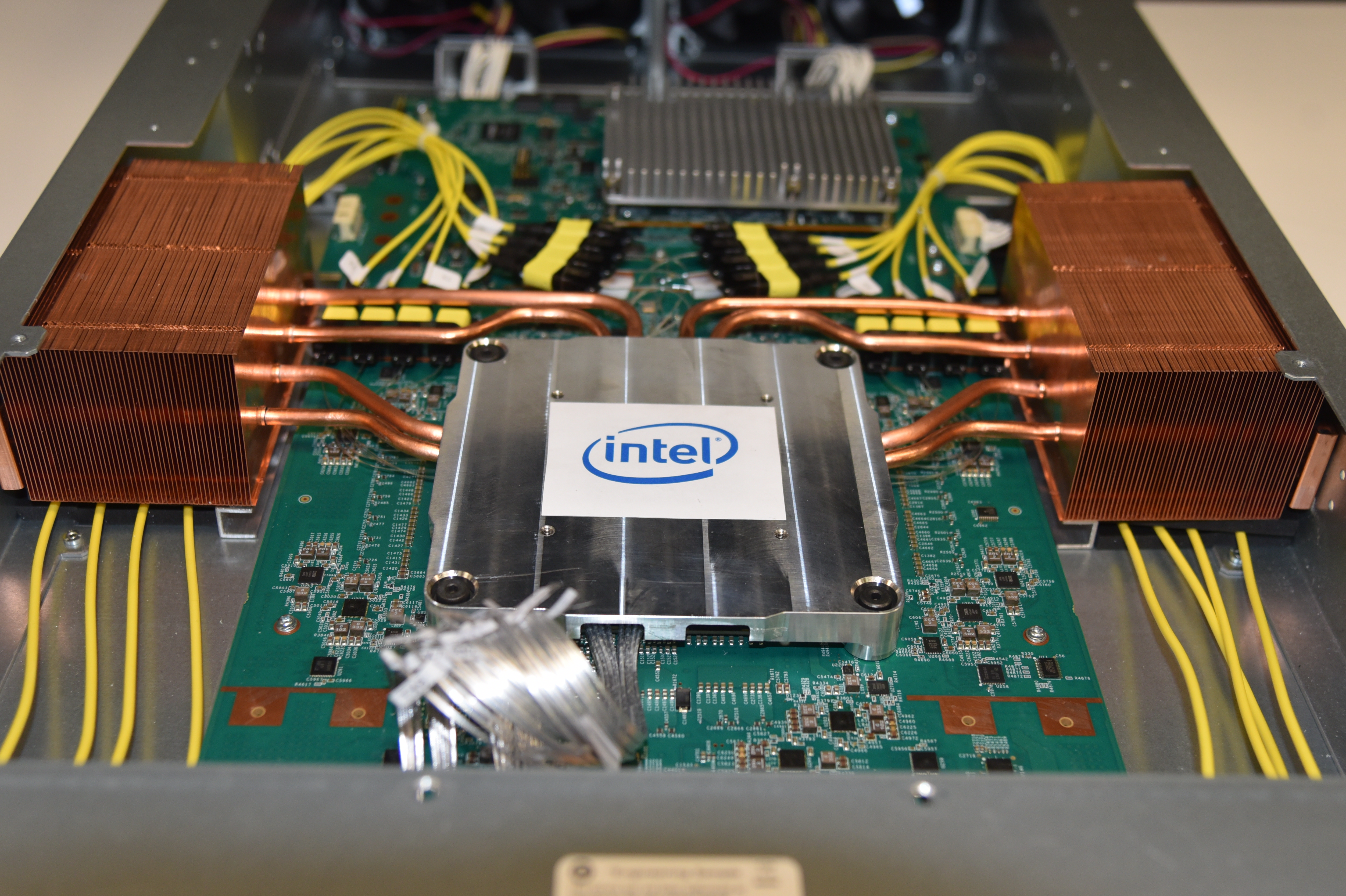
Intel Co-Packaged Ethernet Switch (source: Intel)
The switch has 8 traditional QSFP28 front panel ports and 8 single mode MPO connectors (four at the left and four at the right). These provide a 400G-DR4 signal, which is 8 x 50G. Inside, each single mode MPO cable is routed under the big copper heat sinks and at the top it seems to be broken out into two MPO cables. So four MPO cables at the left and four at the right. They all split into two resulting in 16 (8x2) MPO cables connected at the top of the co-package.
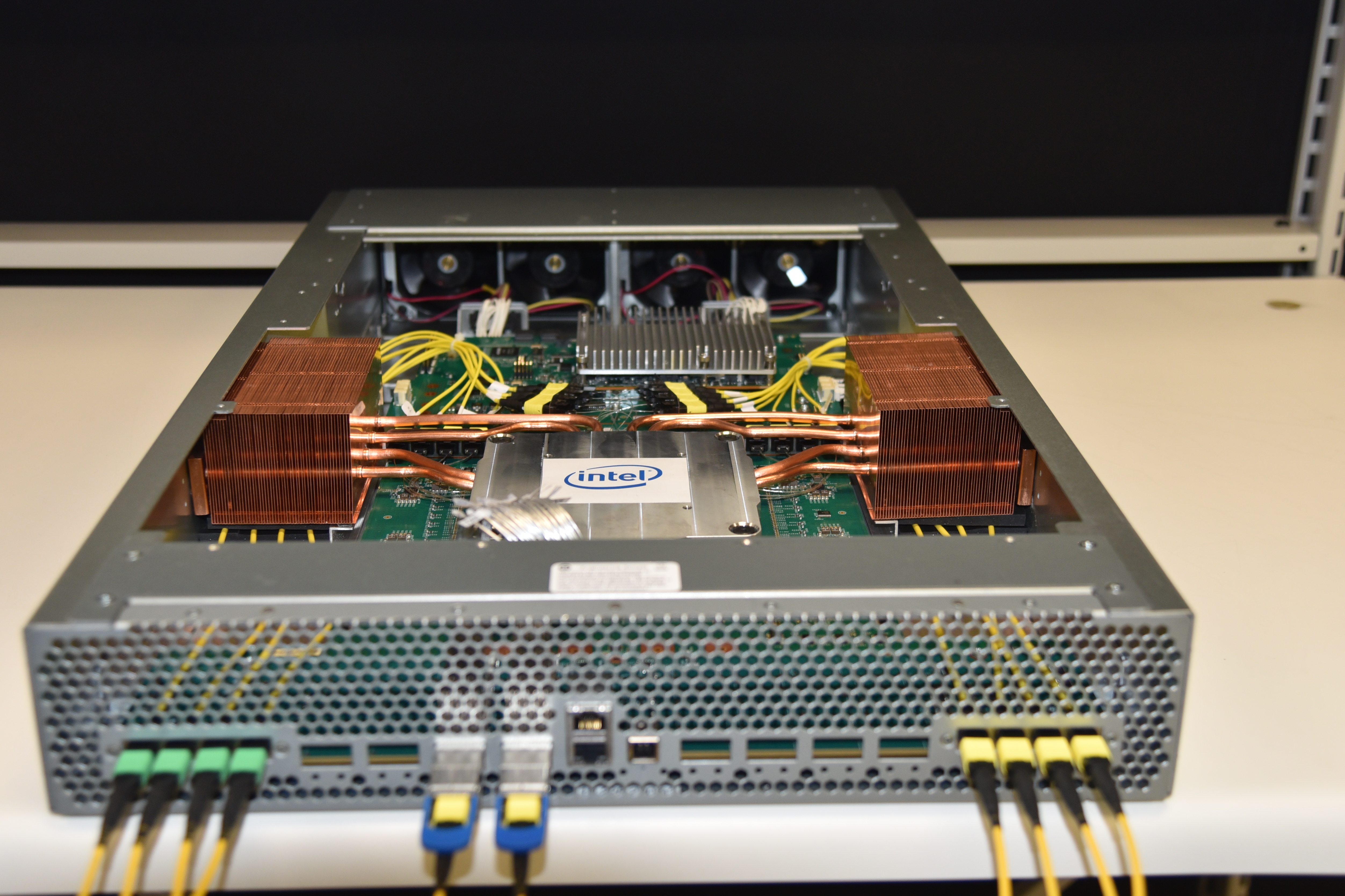
Front panel ports (source: Intel)
It seems like each of the 16 MPO connectors is connected to a small transparant cable, possibly consisting of two strands of fiber (Tx and Rx). These would carry the 50G signals out of the silicon photonics engine.
This is my interpretation of what can be seen in the photos. I have not talked to Intel or Barefoot about the design yet. Please let me know if you have more information or if you think I have it wrong. It is still not clear to me why the MPO cables seem to split in two.
Additional news coverage: Gazettabyte